...
| Pin | Pin | Pin | Pin | Pin | Instructions | ||
|---|---|---|---|---|---|---|---|
| Reinstate POE/ROE mods they are no longer needed. | |||||||
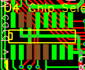
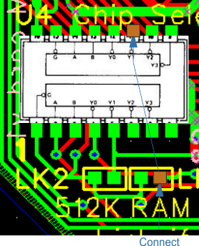
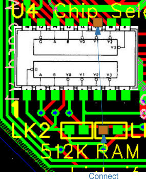
| U4 | 3 | 4 | 5 | 14 | 15 | Lift up pins DO NOT CONNECT TO PCB | |
| U4 | 1 | 2 | 6-8 | 9-13 | 16 | Solder chip to board using the remaining pins | |
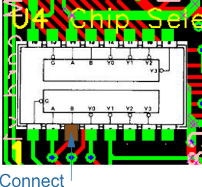
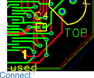
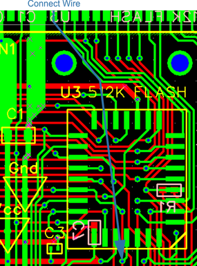
| U4 | 3 | A18 - Connect wire from Pin 3 | |||||
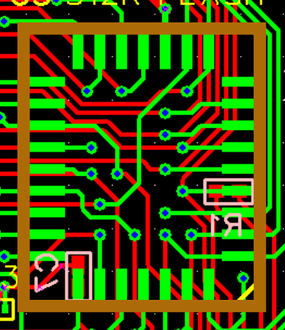
| U1 | to via near 1 U1 | ||||||
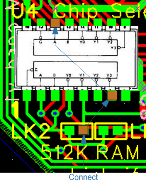
| U4 | 7 | 14 | Connect wire from Pin 7, 14 to RH pad of 512K | ||||
| U4 | 11 | Connect to RH pad of RAM NOTE: This is for the RAM. | |||||
| U3 | Fit socket for U3 | ||||||
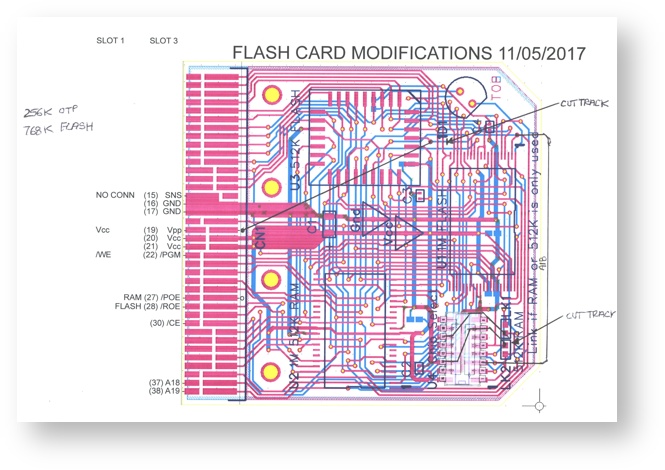
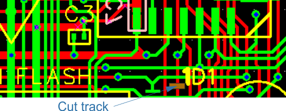
| U3 | 1 | Cut track (A18) | |||||
| U3 | 1 | Connect to Vpp Edge connector Pin 19 | |||||
| LK1 - LK2 |
256K OTP EPROM 768 FLASH Modifications
| Pin | Pin | Pin | Pin | Pin | Instructions | ||
|---|---|---|---|---|---|---|---|
| Reinstate POE/ROE mods they are no longer needed. | |||||||
| U4 | 3 | 4 | 5 | 14 | 15 | Lift up pins DO NOT CONNECT TO PCB | |
| U4 | 1 | 2 | 6-8 | 9-13 | 16 | Solder chip to board using the remaining pins | |
| U4 | 3 | A18 - Connect wire to | |||||
| U1 | via near 1 U1 | ||||||
| U4 | 7 | 14 | Connect to RH pad of 512K | ||||
| U4 | 11 | Connect to LH pad of RAM | |||||
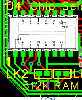
| LK1 - LK2 | Cut track between LH pad of 512 and LH pad of RAM | ||||||
| U3 | Fit socket for U3 | ||||||
| U3 | 1 | Cut track (A18) | |||||
| U3 | 1 | Connect to Vpp Edge connector Pin 19 |
...
