...
The Z88 Flash/RAM card has been working for several years now. When OZ 4.6 was introduced, allowing applications to be run in RAM, some games failed to run.
| Standard VersionDecoder and PROM socket | RAM Version | FLASH Version |
|---|---|---|
|
|
|
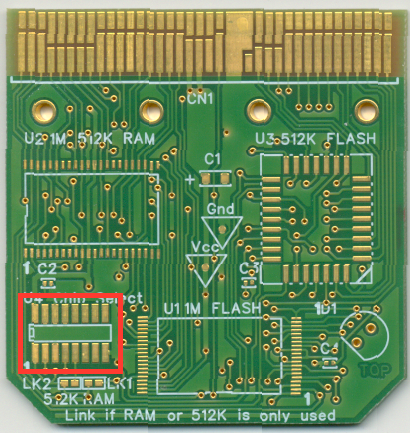
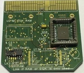
This was thought to be due to an intermittent timing error from the decode chip CD74HCT139 which switches between the RAM and Flash chip but after the Z88 Hardware Investigation, it has been discovered to be a misunderstanding by both the hardware and software engineers on how to write faultlessly to the flash chip. This has only affected a few users, i.e. those who play games in RAM or who do repetitive writing to the flash card. The majority of users have not reported any problems.
...
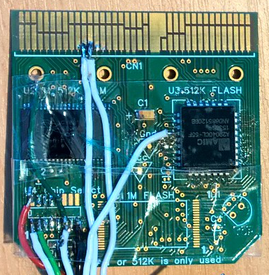
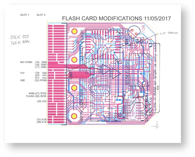
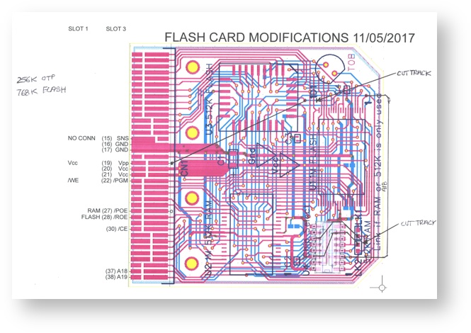
256K OTP EPROM 768 RAM Modifications follows
| Step | Pin | Pin | Pin | Pin | Pin | Instructions | ||||||
|---|---|---|---|---|---|---|---|---|---|---|---|---|
| Reinstate POE/ROE mods they are no longer needed. | ||||||||||||
| 1 |
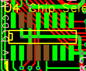
| U4 | 3 | 4 | 5 | 14 | 15 | Lift up pins DO NOT CONNECT TO PCB | ||||
| 2 |
| U4 | 1 | 2 | 6-8 | 9-13 | 16 | Solder chip to board using the remaining pins | ||||
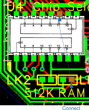
| 3a |
| U4 | 3 | A18 - Connect wire from U4 Pin 3 to (See step 3b) | ||||||||
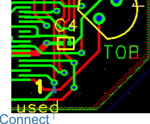
| 3b |
| U1 | to a via near 1 U1U1. (Above the d in 'used' and to the RH side of the figure 1). | |||||||||
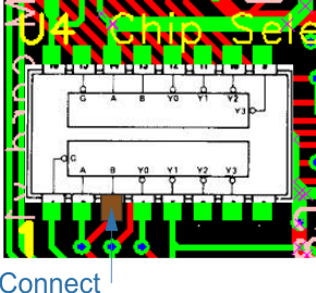
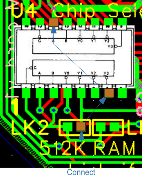
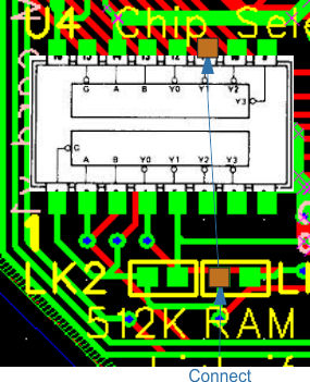
| 4 |
| U4 | 7 | 14 | Connect wire from Pin 7, 14 to RH pad of 512K | |||||||
| 5 |
| U4 | 11 | Connect to RH pad of RAM NOTE: This is for the RAM. | ||||||||
| 6 |
| U3 | Fit socket for U3 |
| U3 | 1 | Cut track (A18) Lift off Pin 1 | |||||
| U3 | 1 | Connect to Vpp Edge connector Pin 19 | |||||||||
| LK1 - LK2 |

256K OTP EPROM 768 FLASH Modifications follow
| Step | Pin | Pin | Pin | Pin | Pin | Instructions | ||||||
|---|---|---|---|---|---|---|---|---|---|---|---|---|
| Reinstate POE/ROE mods they are no longer needed. | ||||||||||||
| 1 |
| U4 | 3 | 4 | 5 | 14 | 15 | Lift up pins DO NOT CONNECT TO PCB | ||||
| 2 |
| U4 | 1 | 2 | 6-8 | 9-13 | 16 | Solder chip to board using the remaining pins | ||||
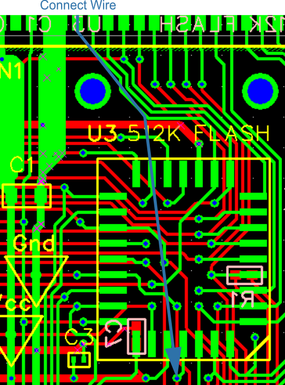
| 3a |
| U4 | 3 | A18 - Connect wire | ||||||||
| 3b |
| U1 | to a via near 1 U1U1. (Above the d in 'used' and to the RH side of the figure 1). | |||||||||
| 4 |
| U4 | 7 | 14 | Connect to RH pad of 512K | |||||||
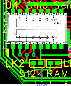
| 5 |
| U4 | 11 | Connect to LH pad of RAM | ||||||||
| 6 |
| LK1 - LK2 | Cut track between LH pad of 512 and LH pad of RAM | |||||||||
| 7 |
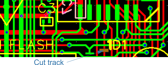
| U3 | Fit socket for U3 |
| U3 | 1 | Cut track (A18) DO NOT connect Pin 1 (Bottom row middle pin) to the PCB. Lift off the pin to connect the wire at the next step. | |||||
| 8 |
| U3 | 1 | Connect wire from the lifted off Pin 1 U3, to Vpp Edge connector Pin 19 |
...