...
| Table of Contents |
|---|
Introduction
...
The Z88 Flash/RAM card has been working for several years now. When OZ 4.6 was introduced, allowing applications to be run in RAM, some games failed to run.
| Standard Version | Modified Turbo Version |
|---|---|
|

This was found to be due to an intermittent timing error from the decode chip CD74HCT139 which switches between the RAM and Flash chip.
Although this is one of the fastest decode chips, it is too slow for our purposes.
The Z88 only uses one half of this dual decode chip. This circuit may be made with
- 3 inverters
- 2 NAND gates
The inverters are slower than the NAND gates, so it was decided to use 5 NAND gates using 3 of the gates as inverters.taking 10nS, the software speed improvements pushed it outside these limits.
This documents the steps taken to rectify this. The detail of the steps taken are in subsections, allowing the reader to go into detail if required.
Object
The object of this exercise is to see if by redefining the design on a small PCB, with the same footprint (SMD SO16) of the existing decode chip, a faster decode could be achieved by
...
- Using high speed NAND gates, to see if then if that was successful
...
- Use a decode chip from the same family.
Choosing a Fast NAND gate
Looking through the datasheets for NAND gates found the following timings:-
...
SOT-23-5
...
The Single 2-input Positive NAND gates display the fastest times.
Here is the chip that has been chosen:-


Circuit Description
There are 2 inputs,
- A19 - Selects either the top half of the 1M memory space for the flash chip or the bottom half for the RAM.
- /CE - Selects the 1M card.
Truth Table of the 74139
...
A1
GND
...
Logic Diagram
Original

Cut Down Version using two inputs and two outputs
This ignores A1 GND line.

Logic Lab Test v Truth Table
The logic was checked with thanks to http://www.neuroproductions.be/logic-lab/ for the simulator.
...
00

01

02

03

They both agree.
Circuit Diagram
Circuit updated 15:04 6/9/16

Can a Full 74139 chip be built?
The Z88 only uses one half of the dual functionality of the full chip.
Using just NAND gates requires too many of them. See http://www.neuroproductions.be/logic-lab/index.php?id=63191 for the unfinished work in getting a full chip to work.
Building a prototype board internally
A prototype board was built inside the Flash card..

07/09/16
...
- Using the knowledge gained, add more components to make a high speed 74xx139 card.
NAND Gate Build
Building the circuit on a breadboard externally
Components required
...

...

10 sot to IC adaptors were obtained in addition to the 5 NAND gates . The circuit could now be bread-boarded and tested outside the Z88 card case.

The four signal and power lines can be seen connecting the card to the breadboard.

Plan view showing all the connections.
Oscilloscope Readings

This produced the signals required.
This trace shows the Flash chip being selected (/CE1) in 3nS.
The RAM (/CE) would be the same timings.
...
| title | Signals not the same abbreviations as the circuit |
|---|
The names of the signals on the scope are not all the same as shown in the circuit.
...
Printed Circuit Board
A PCB has been laid out (just in case Tony's prototype works).
Main points
- A letterbox slot has been made in the centre of the HD1, HD2, (which are connected both sides,) so that either direct soldering or wire links may be used to connect the signals from the 512K/512K card to the PCB.
- The pads of the footprint of the SOT-23-5 have been made longer, to enable easier soldering of the small parts.
- The bottom Left Hand corner of the PCB matches the shape of the 512K/512K Card for easy alignment.
- C2 on the 512K/512K, needs to be removed and put onto the PCB, in the same space. This is to make the PCB a bit larger for stability.
The 7 layers
Here are the layers printed on A4 sheets. The board is small, zooming in is generally helpful.
(updated 19:16 07/09/2016)
| View file | ||||
|---|---|---|---|---|
|
were used to test whether a faster time could be achieved with the Z88.
Results
The latest software was tried again in a standard 512K/512K Flash/RAM Card and Vic could not make the games software go wrong. The prototype board was packed and sent to Mr T who had a failing Z88 and 512K/512K Flash/RAM Card. He confirmed that it was the decoder chip that was causing the fault and suggested that another decoder could be found.
...
DECODER
...
Chip Build
Looking through the datasheets for a Texas Instruments VC1 chip found the following timings:-
...
SN74LVC1G139DCTR
...
The 2-to-4 Line Decoder display fast times.
Here is the chip that has been chosen:-
...

| PART NUMBER | PACKAGE | BODY SIZE (NOM) |
|---|---|---|
| SN74LVC1G139DCT | SM8 (8) | 2.95 mm × 2.80 mm |
| SN74LVC1G139DCU | VSSOP (8) | 2.30 mm × 2.00 mm |
...
Circuit Description
There are 2 inputs,
- A19 - Selects either the top half of the 1M memory space for the flash chip or the bottom half for the RAM.
- /CE - Selects the 1M card.
Truth Table of Decode Chip
...
Circuit Diagram
Circuit not drawn yet
Building the circuit on a breadboard externally
Components required
...

...
...
Building the circuit on a breadboard externally
Using 5 NAND Gates to prove that there is a hardware problem was very useful, but for a production run using a single 2-to-4 Line Decoder chipschip to replace them is the next step.
This circuit could now be bread-boarded and tested outside the Z88 card case again.

The four signal and power lines can be seen connecting the card to the breadboard.
Plan view showing all the connections.
Oscilloscope Readings
This produced the signals required.
This trace shows the Flash chip being selected (/CE1) in 3nS.
The RAM (/CE) would be the same timings.
...
| title | Signals not the same abbreviations as the circuit |
|---|
The names of the signals on the scope are not all the same as shown in the circuit.
...
Printed Circuit Board
A PCB has been laid out (just in case Tony's prototype works).
Main points
- A letterbox slot has been made in the centre of the HD1, HD2, (which are connected both sides,) so that either direct soldering or wire links may be used to connect the signals from the 512K/512K card to the PCB.
- The pads of the footprint of the SOT-23-5 have been made longer, to enable easier soldering of the small parts.
- The bottom Left Hand corner of the PCB matches the shape of the 512K/512K Card for easy alignment.
- C2 on the 512K/512K, needs to be removed and put onto the PCB, in the same space. This is to make the PCB a bit larger for stability.
The 7 layers
Here are the layers printed on A4 sheets. The board is small, zooming in is generally helpful.
(updated 19:16 07/09/2016)
View file

Results
The Games played without crashing. The PCB could now be designed.
Z88 Turbo Card produced
It has been proved that the decode chip in the Z88 Flash/RAM card is too slow. Existing users who wish to run applications in RAM will need their cards modified with the chip being replaced with this card.
Full 74xx139 Version Build Concept
A new opportunity or a waste of time?
The decoder chip above works. It changes the timing from 10 to 3nS and replaces 1/4 of the 74139 in the Z88 design. Is there a demand for a full 74xx139 replacement card?
For the full version, adding 2 OR, dual logic gates to the outputs adds the /CE signal to the design. The challenge is to
- fit 6 chips into a 16 pin DIL footprint
- establish whether there is a demand
SMD or DIL Footprint?
| 16 pin DIL | 16 pin SO 16 |
|---|---|
|
|
| |

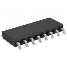

Using the Z88 Turbo Card fitting pins or wires to connect the 74xx139 Card piggybacked both footprints may be accommodated. This has proved to be impractical. Another design needs to be considered if required perhaps using a slot across the middle to connect the SO16 footprint to the card.
Build 74xx139 on a 16 pin DIL footprint
This should be possible, 3 chips on each side of the PCB with 2 rows of 8 pins on either side.
Demand or not?
Once the PCB design has been completed, it can be costed and this concept can be floated.
A decision may be made then whether to proceed with manufacture the PCB or not. It could be used in legacy equipment to see if it improved the performance. There could also be different options.
- card only
- card and components (to build)
- fully built
It will definitely not be able to compete on price, as it will cost more than 10p.
Building the circuit on a breadboard externally
Needs to be done
A test needs to be done to test the functionality of the NAND gate using the /CE signal.

The four signal and power lines can be seen connecting the card to the breadboard.

Results
The results need to be reported.
Printed Circuit Board
74xx139 DIL Card
To be done

There are two functions for this card.
- The DIL 16 pads have holes through them allowing wires to be soldered to DIL 16 pads on another card.
- When used with the Z88 Flash/RAM card, it can be used with a SO 16 footprint. 16 pins or wires need to be soldered so that the DIL chip or converter card can be piggy backed on top with 2 off SIL sockets.
74xx139 to be produced or not
Depends on response.