...
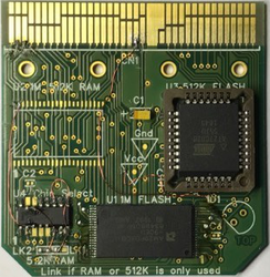
The Z88 Flash/RAM card has been working for several years now. When OZ 4.6 was introduced, allowing applications to be run in RAM, some games failed to run.
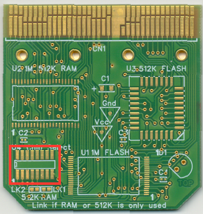
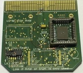
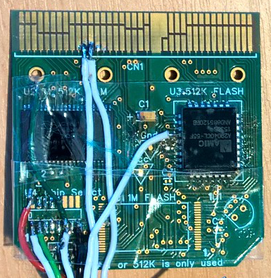
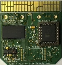
| Standard VersionDecoder and PROM socket | RAM Version | FLASH Version |
|---|---|---|
This was thought to be due to an intermittent timing error from the decode chip CD74HCT139 which switches between the RAM and Flash chip but after the Z88 Hardware Investigation, it has been discovered to be a misunderstanding by both the hardware and software engineers on how to write faultlessly to the flash chip. This has only affected a few users, i.e. those who play games in RAM or who do repetitive writing to the flash card. The majority of users have not reported any problems.
...
The modified 512K/512K card has already been used with the modified extender card as described in the Z88 Hardware Investigation section, to test how the decoder chip may be used with different address maps. It was decided just to build a card using the knowledge gained from these previous tests.
Decoder Details
...
The same decoding algorithm is used for both cards. The output is either connected to the CE of the RAM or FLASH chip.
256K OTP EPROM, 768K FLASH or RAM
| CE | A19 | A18 | |
|---|---|---|---|
| 256K OTP EPROM | 0 | 1 | 1 |
| 768K FLASH or RAM | 0 | 1 | 0 |
| 768K FLASH or RAM | 0 | 0 | 1 |
| 768K FLASH or RAM | 0 | 0 | 0 |
| NOT SELECTED | 1 | X | X. |
Decoder Connections
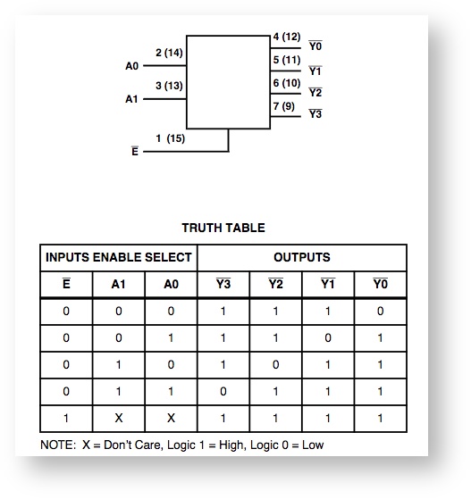
The decode chip used, is repeated twice in the same device. The first part does the 256K chip select device decodes the 256K EPROM with SE1, A19 and A18. The unused decode decoder is then used to decode select the remainder of the address space, when the card is selected but not the 256K EPROM. The output going to either the RAM or FLASH chip enable.
Selecting the decoder outputs
...
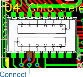
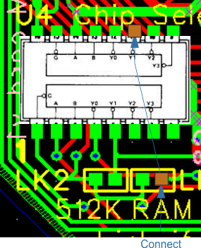
The output for the RAM or Flash is Y1 (Pin 11).
Connecting the OTP EPROM
U3 Variants
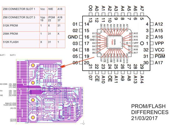
U3 is currently wired up for a 512K Flash chip. There are 3 signals that use 2 different pins on the PLCC footprint.
These are displayed in the following table.
If links are to be used on a future designed board the following layout maybe considered
| From edge connector | Vpp (19) | A18 (37) | /PGM (22) | ||
|---|---|---|---|---|---|
| To U3 PLCC Footprint | Pin 1 | Pin 31 | |||
| 512K PROM | |||||
| 256K PROM | |||||
| 512k FLASH |
The 256K PROM is being used
Vpp needs to be connected to pin 1
PGM is already connected to pin 31
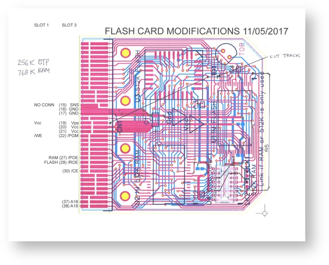
PCB Modifications
Connection Chart
| Edge Con | Decoder | Signal | OTP EPROM | 1M RAM | 1M Flash | |
|---|---|---|---|---|---|---|
| 30 | 1 | SE1 | EXISTING CONNECTION | |||
| 38 | 2 | A19 | EXISTING CONNECTION | |||
| 37 | 3 | A18 | ||||
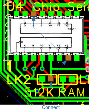
| 7 | 14 | OTP CE | 22 | RH 512K LK | RH 512K LK | |
| 11 | RAM CE | RH RAM LK | ||||
| 11 | FLASH CE | LH RAM LK | ||||
256K OTP EPROM 768 RAM Modifications follows
| Step | Pin | Pin | Pin | Pin | Pin | InstructionInstructions | ||
|---|---|---|---|---|---|---|---|---|
| Reinstate POE/ROE mods they are no longer needed. | ||||||||
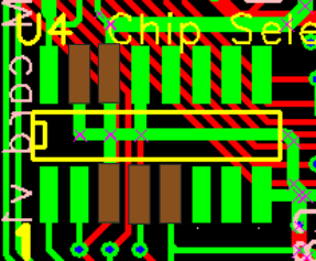
| 1 | U4 | 3 | 4 | 5 | 14 | 15 | Lift up pins DO NOT CONNECT TO PCB | |
| 2 | U4 | 1 | 2 | 6-8 | 9-13 | 16 | Solder chip to board using the remaining pins | |
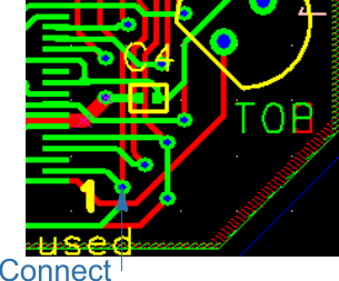
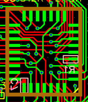
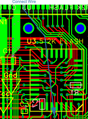
| 3a | U4 | 3 | A18 - Connect to pad near 1 U1wire from U4 Pin 3 to (See step 3b) | |||||
| 3b | U1 | to a via near U1. (Above the d in 'used' and to the RH side of the figure 1). | ||||||
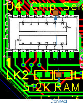
| 4 | U4 | 7 | 14 | Connect wire from Pin 7, 14 to RH pad of 512K | ||||
| 5 | U4 | 11 | Connect to RH pad of RAM NOTE: This is for the RAM. | |||||
| 6 | U3 | Fit socket for OTP EPROMU3 Lift off Pin 1 | ||||||
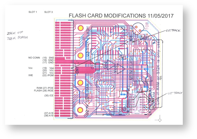
| Cut track (A18) | U3 | 1 | Connect to Vpp Edge connector Pin 19 | |||||
| LK1 - LK2 |
256K OTP EPROM 768 FLASH Modifications follow
| Step | Pin | Pin | Pin | Pin | Pin | InstructionInstructions | ||||
|---|---|---|---|---|---|---|---|---|---|---|
| Reinstate POE/ROE mods they are no longer needed. | ||||||||||
| 1 | U4 | 3 | 4 | 5 | 14 | 15 | Lift up pins DO NOT CONNECT TO PCB | |||
| 2 | U4 | 1 | 2 | 6-8 | 9-13 | 16 | Solder chip to board using the remaining pins | |||
| 3a | U4 | 3 | A18 - Connect to pad near 1 U1wire | |||||||
| 3b | U1 | to a via near U1. (Above the d in 'used' and to the RH side of the figure 1). | ||||||||
| 4 | U4 | 7 | 14 | Connect to RH pad of 512K | ||||||
| 5 | U4 | 11 | Connect to LH pad of RAM | |||||||
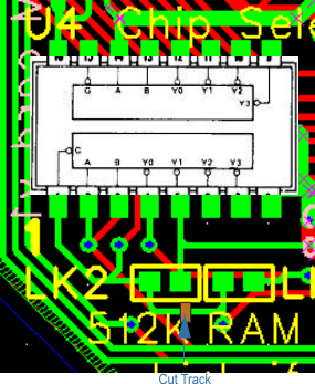
| 6 | LK1 - LK2 | Cut track between LH pad of 512 and LH pad of RAM | ||||||||
| 7 | U3 | Fit socket for OTP EPROMU3 | 1 | Cut track (A18) DO NOT connect Pin 1 (Bottom row middle pin) to the PCB. Lift off the pin to connect the wire at the next step. | ||||||
| 8 | U3 | 1 | Connect wire from the lifted off Pin 1 U3, to Vpp Edge connector Pin 19 |
...
