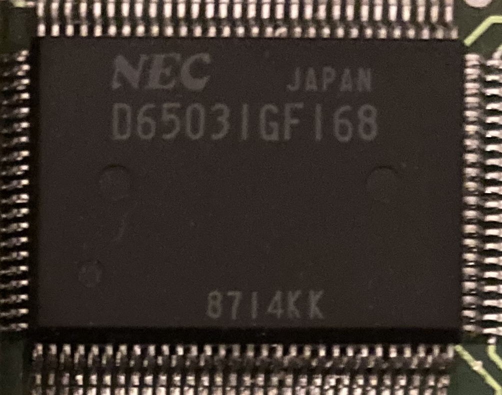
The Blink gate-array is a custom ASIC : NEC D65031GF168. This SMD is a uPD65000 series (low power 2 micron ASIC) with 138 rows of 24 columns, 3312 cells of 4 transistors.
GF stands for a flat packaging of 100 pins. 168 is the circuit type number identifying the blink design.
It contains the logic of :
the memory management unit (MMU)
the real time clock (RTC)
the Z80 clock and power management
the Z80 reset
the programmable interrupt controller (PIC)
the UART
the LCD controller
the EPROM programmmer
the speaker
Pin     Name    Type    Description
1       GND     -       Ground
2       VDD     -       +5V
3       IOR     I       Z80 /IORQ
4       CRD     I       Z80 /RD
5       MRQ     I       Z80 /MREQ
6       HLT     I       Z80 /HALT
7       NMIB    O       Z80 /NMI
8       INTB    O       Z80 /INT
9       CDB     IO      Z80 D1
10      ROUT    O       Z80 /RST
11      CDA     IO      Z80 D0
12      CM1     I       Z80 /M1
13      CDH     IO      Z80 D7
14      CDC     IO      Z80 D2
15      CA0     O       Z80 A0
16      CDG     IO      Z80 D6
17      CA1     O       Z80 A1
18      CDF     IO      Z80 D5
19      CA2     O       Z80 A2
20      CDD     IO      Z80 D3
21      CA3     O       Z80 A3
22      CDE     IO      Z80 D4
23      CA4     O       Z80 A4
24      CA5     O       Z80 A5
25      CA15    O       Z80 A15
26      CA6     O       Z80 A6
27      CA14    O       Z80 A14
28      GND     -       Ground
29      VDD     -       +5V

30      CA13    O       Z80 A13
31      CA7     O       Z80 A7
32      CA8     O       Z80 A8
33      CA12    O       Z80 A12
34      CA9     O       Z80 A9
35      CA11    O       Z80 A11
36      CA10    O       Z80 A10
37      TxD     O       UART TXD
38      RTS     O       UART RTS
39      IRCE    O       RAM.0 /CE
40      GND     -       Ground
41      RxD     I       UART RXD
42      CTS     I       UART CTS
43      DCD     I       UART DCD
44      PM1     O       Z80 clock (3.2768 MHz)
45      LP      O       LCD control, 10ms  line pulse
46      FR      O       LCD control, 156us frame
47      XSCL    O       LCD control, 300ns data
48      LD0     O       LCD data
49      LD1     O       LCD data
50      LD2     O       LCD data
51      LD3     O       LCD data

52      VDD     -       +5V
53      GND     -       Ground
54      MA16    O       Memory A16
55      MA15    O       Memory A15
56      MA14    O       Memory A14
57      MA12    O       Memory A12
58      MA7     O       Memory A7
59      MA13    O       Memory A13
60      MA6     O       Memory A6
61      MA8     O       Memory A8
62      MA5     O       Memory A5
63      WRB     O       Write enable /WE
64      MA9     O       Memory A9
65      MA4     O       Memory A4
66      MA11    O       Memory A11
67      MA3     O       Memory A3
68      IPCE    O       ROM.0 /CE
69      MA2     O       Memory A2
70      MA10    O       Memory A10
71      MA1     O       Memory A1
72      MA0     O       Memory A0
73      MDH     IO      Memory D7
74      MDA     IO      Memory D0
75      MDG     IO      Memory D6
76      MDB     IO      Memory D1
77      MDF     IO      Memory D5
78      MDC     IO      Memory D2
79      VDD     -       +5V
80      GND     -       Ground

81      MDE     IO      Memory D4
82      MDD     IO      Memory D3
83      MA17    O       Memory A17
84      MA18    O       Memory A18
85      MAW     O       Memory A19
86      SE1     O       Slot1 /CE
87      POE     O       PSRAM /OE (refreshed)
88      ROE     O       ROM /OE
89      PGMB    O       Slot 3 /WE (Program Byte)
90      EOE     O       Slot 3 /OE (Eprom OE)
91      SE3     O       Slot 3 /CE
92      FLP     I       Flap
93      SE2     O       Slot2 /CE
94      SNS     I       Sens line (card insertion)
95      VPON    O       VPP on
96      BTL     I       Batt low
97      RIN     I       Reset input
98      MCK     I       Master clock (9.8304 MHz)
99      SCK     I       Standby clock (25.6 KHz)
100     SPKR    O       speaker
The original notes as supplied to Cambridge Computer were lost during the time of the company's move from Cambridge to Scotland.
SNS
Card insertion or removal is detected by SNS. This feature was patented by James Westwood (#WO8809573, 1988-12-01). When SNS goes low, an NMI is fired and initiate a shutdown. This prevent any loss off data or system crash.
POE, ROE, EOE, pseudo-static RAM refresh
POE : Pseudo-static OE
ROE : Rom OE
EOE : Eprom OE
When Z80 is running and LCD is on, the refresh is performed by the LCD controller reading the memory.
When LCD is off (DOZE state), the 42832 is not in standby mode, it needs to be refreshed.
POE provides this refresh, ROE does not. POE is tracked to slot 0 RAM, slot 1 and slot 2 connectors.
Pseudo static RAM card are not supported in slot 3. The POE line in slot 3 connector is replaced by the EOE. EOE is driven by the EPR register.
Z80 Refresh signal is not wired. Refresh logic in blink is done from CRD, CM1, MRQ (negative signals) :
POE = ROE | ( CRD & ~CM1 & ~MRQ)
Clocks and power management
Z80 clock (PM1) is driven by the Blink, the CMOS Z80 can be stopped without losing register state.
Active : PM1 = MCK / 3 = 9.8304 / 3 = 3.2768MHz
Snooze : PM1 is stopped
Coma : PM1 = SCK = 25.6KHz
Master clock is 9.83MHz because LCD controller has to read screen files in memory.
LCD controller
A 640 bits shift register is used to build the current line and shift nibbles to the LCD data lines.
The LCD frame rate is 100Hz, one page every 10ms (LP).
One line is sent every 156.25us (FR). A burst of 160 nibbles at 3.2768 MHz (300ns period) are sent. It last 48us and is followed by a 108.25us inactive period.