...
| CE | A19 | A18 | |
|---|---|---|---|
| 256K OTP EPROM | 0 | 1 | 1 |
| 768K FLASH or RAM | 0 | 1 | 0 |
| 768K FLASH or RAM | 0 | 0 | 1 |
| 768K FLASH or RAM | 0 | 0 | 0 |
| NOT SELECTED | 1 | X | X. |
Decoder Connections
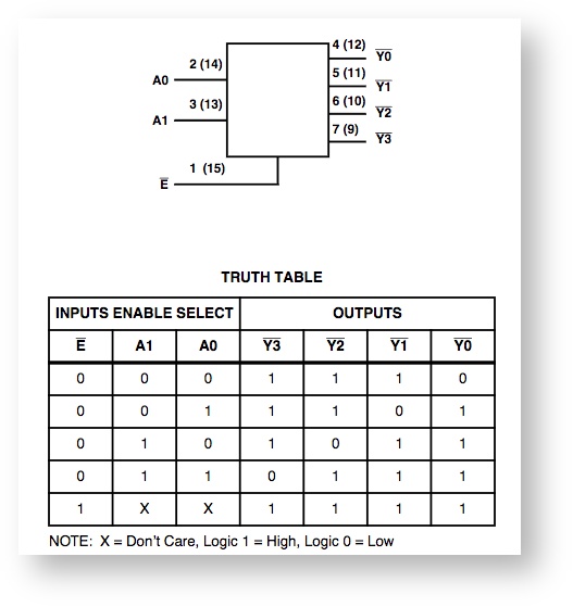
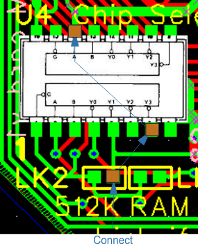
The decode chip used, is repeated twice in the same device. The first device decodes the 256K EPROM with SE1, A19 and A18. The unused decoder is used to select the remainder of the address space, when the card is selected but not the 256K EPROM. The output going to either the RAM or FLASH chip enable.
...
| Pin | Pin | Pin | Pin | Pin | Instructions | ||
|---|---|---|---|---|---|---|---|
| Reinstate POE/ROE mods they are no longer needed. | |||||||
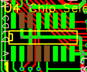
| U4 | 3 | 4 | 5 | 14 | 15 | Lift up pins DO NOT CONNECT TO PCB | |
| U4 | 1 | 2 | 6-8 | 9-13 | 16 | Solder chip to board using the remaining pins | |
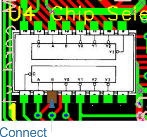
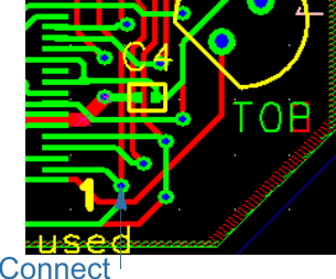
| U4 | 3 | A18 - Connect wire from Pin 3 | |||||
| U1 | to via near 1 U1 | ||||||
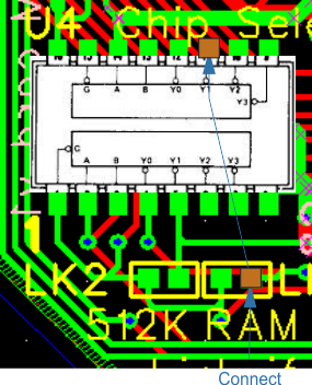
| U4 | 7 | 14 | Connect wire from Pin 7, 14 to RH pad of 512K | ||||
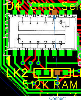
| U4 | 11 | Connect to RH pad of RAM NOTE: This is for the RAM. | |||||
| U3 | Fit socket for U3 | ||||||
| U3 | 1 | Cut track (A18) | |||||
| U3 | 1 | Connect to Vpp Edge connector Pin 19 | |||||
| LK1 - LK2 |
...
| Pin | Pin | Pin | Pin | Pin | Instructions | ||
|---|---|---|---|---|---|---|---|
| Reinstate POE/ROE mods they are no longer needed. | |||||||
| U4 | 3 | 4 | 5 | 14 | 15 | Lift up pins DO NOT CONNECT TO PCB | |
| U4 | 1 | 2 | 6-8 | 9-13 | 16 | Solder chip to board using the remaining pins | |
| U4 | 3 | A18 - Connect wire to | |||||
| U1 | via near 1 U1 | ||||||
| U4 | 7 | 14 | Connect to RH pad of 512K | ||||
| U4 | 11 | Connect to LH pad of RAM | |||||
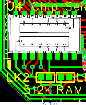
| LK1 - LK2 | Cut track between LH pad of 512 and LH pad of RAM | ||||||
| U3 | Fit socket for U3 | ||||||
| U3 | 1 | Cut track (A18) | |||||
| U3 | 1 | Connect to Vpp Edge connector Pin 19 |
...

