Table of Contents
...
This document forms the basis of a collaborative project between anyone who wishes to be involved.
NOTE: The Z88 Motherboard PCB section was not completed. Please go to Articles on Modifying Motherboards
Discussion Section
Here is the section where you can discuss different topics
...
The following table illustrates this.
...
| Name of Input Device | Header | Z88 Input Chip | Input | Additional Target Signals | Name of Target Device | Target Chip | Target Footprint | ||||||
|---|---|---|---|---|---|---|---|---|---|---|---|---|---|
ROM LH side | NEC 128K 8-bit static CMOS ROM. It is packaged in a 600-mil, 32-pin plastic DIP. | 2x16 SIL | uPD23C1001E | A0 - A16 D0 - D7 /CE /OE | A17 A18 | AMIC A29040CL-55F | AMIC A29040CL-55F | PLCC-32 Socket | |||||
RAM RH side | NEC x8 Pseudo Static RAM (32K) | 2x16 SIL | uPD42832C | A0 - A16 | A17 A18 | BS62LV8001EIP55 IC, | BS62LV8001EIP55 | 44-pin TSOP II | |||||
| SIL header | 3x1SIL | A17 A18 /CE Slot 1 |
Signals that are not used will be ignored.
...
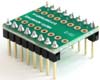
 | 32 pin SOIC to DIL PCB |  | PLCC - 32 to DIL PCB |
 | 44 pin tsop to DIL PCB |  | SOP - 36 to DIL PCB |
| DIP-16 (0.3" body) to DIP-16 (0.6" body) adaptor (TH mount bottom pins) x 4 |
PCB footprint converters for the proposed chips have been ordered from Canada.
...
The chips may not be manufactured any more but you may still find vintage parts suppliers being able to supply the on E bay -Bay and Chinese sites.

| |
 |


...

Component side of board.
To use JEDEC EPROM for internal ROM:Disconnect IC3 pin 2 from the ROE track by cutting it in two places on the component side of the board. The adjacent A16 track is shown for clarity because the view is usually obscured by a socket. Disconnect IC3 pin 24 from the A16 track by cutting it on the solder side of the board. Connect IC3 pin 24 to the ROE pad close to IC3 pin 17. Connect the ROE pad close to IC3 pin 31 to the ROE track going to SLOT 1. Connect IC3 pin 2 to the A16 track going to SLOT 2.To use 256K JEDEC EPROM for internal ROM:Also disconnect IC3 pin 30 from VCC by cutting the track from pin 31. Connect IC3 pin 30 to the A17 track going to slot 2 pin 36. 128K JEDEC EPROM should still work but is not tested.To use 512K JEDEC EPROM for internal ROM:Also disconnect IC3 pin 31 from VCC by cutting the track from pin 32. Connect IC3 pin 31 to the A18 track going to slot 2 pin 37. Not sure if 128K or 256K JEDEC EPROM can be used after this modification because of pin 31 /PGM. For layout of code on larger than 128K internal ROMs see: Z88 Internal ROM Modifications

Solder side of board.
To use 128K static RAM for internal RAM: No track changes needed.To use 512K static RAM for internal RAM:Disconnect IC2 pin 30 from the VCC by cutting the track from pin 32. Connect IC2 pin 30 to A17 at slot 2 pin 36. Disconnect IC2 pin 31 from the /PGM track by cutting it close to the pad near pin 1 and 2. Connect the IC2 pin 31 to A18 at slot 2 pin 37. Not sure if 128K static RAM can be used after this modification because of pin 30 CS2.
...
| Warning | ||
|---|---|---|
| ||
Unable to select Slot 0. 1, 2 and 3 work. |
or you could send the chip to Rakewell who can program it for you.