Motherboard Modifications
Z88 Motherboard PCB
Introduction
This document forms the basis of a collaborative project between anyone who wishes to be involved.
NOTE: The Z88 Motherboard PCB section was not completed. Please go to Articles on Modifying Motherboards
Discussion Section
Here is the section where you can discuss different topics
Object
Rather than
- build the Z88 using obsolete parts that were used in the articles below,
- cutting tracks on the old Z88 motherboard,
- bending chip pins out so they do not connect to the board,
This project aims to build a PCB which has the following specification.
Specification
- 512K Flash replacing the Z88 ROM
- 1M RAM.
- 512K allocated to Slot 0
- 512K allocated to Slot 1 - option
Advantages using a PCB.
- No track modifications need to be made to the Z88 motherboard.
- The original RAM and ROM chips are carefully un-soldered and stored until recovered again..
- They are replaced with 2 off 32 pin, low profile sockets for this PCB to plug into.
- The components used, are the same proven chips that have been used in the 512K/512K Flash/RAM Cards.
- The Flash chip AMIC A29040CL-55F is a PLCC-32 footprint. Fitting a socket, allows the chip to be removed and reprogrammed with an EPROM programmer separately.
- Using a separate adaptor card with another PLCC-32 socket, allows the chip to be reprogrammed with an EPROM ERASER.
- No card connector problems as it is on the other side.
- The Z88 can be returned to its original state, by removing the PCB and replacing the original RAM and ROM chips back into the sockets.
Main Document
General
This board converts the footprint of the Z88 ROM and RAM to the footprint of the new chips. To keep the PCB tracks as short as possible the replacement chips will be over the Z88 ROM area. The only signal from the ROM area is the /CE. All the other signals are obtained from the RAM side.
All data, control, and address lines will be taken directly from the header to the target chip. There are two address lines that need to be collected. A17 and A18. These are located on the Z88 near the Card connector. Thin wires are used here to connect the Z88 to a couple of pins on the PCB.
The following table illustrates this.
| Name of Input Device | Header | Z88 Input Chip | Input | Additional Target Signals | Name of Target Device | Target Chip | Target Footprint | |
|---|---|---|---|---|---|---|---|---|
ROM LH side | NEC 128K 8-bit static CMOS ROM. It is packaged in a 600-mil, 32-pin plastic DIP. | 2x16 SIL | uPD23C1001E | A0 - A16 D0 - D7 /CE /OE | A17 A18 | AMIC A29040CL-55F | AMIC A29040CL-55F | PLCC-32 Socket |
RAM RH side | NEC x8 Pseudo Static RAM (32K) | 2x16 SIL | uPD42832C | A0 - A16 | A17 A18 | BS62LV8001EIP55 IC, | BS62LV8001EIP55 | 44-pin TSOP II |
| SIL header | 3x1SIL | A17 A18 /CE Slot 1 |
Signals that are not used will be ignored.
1M RAM
On the 512K/512K Flash/RAM Card, the unused 512K of RAM is ignored. With this card being able to access all the signals in the Z88, the spare 512K of RAM may be allocated to any of the other card slots, 1 2 or 3 by picking up the /CE signal of that slot.
A card, of the following types, up to 512K may be used in that slot:-
- EPROM
- ROM
- Flash
but no RAM, as that has already been allocated.
Additional Signals connected to the Z88
A SIL header will be used to connect wires for
- A17 and A18, the additional address lines not provided on the headers. These are picked up from the Slot 1 external card connector, pins xx and xx.
- /CE from Slot 1, 2, or 3 to allocate 512K of RAM to that slot.
Points noted
On the Z88 circuit diagram, the RAM is shown on the left and the ROM is shown on the right. Physically, on the Z88, the ROM is on the left and the RAM is on the right.
Building a Prototype Board
PCB Footprint Converters
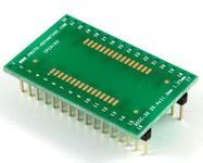
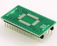
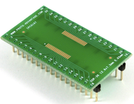
To aid construction, converters will be used for the surface mount RAM, and Flash devices.
DIL or DIP packages are easier to handle and solder connecting wires to.
Here are some examples:-
| 32 pin SOIC to DIL PCB | PLCC - 32 to DIL PCB | ||
| 44 pin tsop to DIL PCB | SOP - 36 to DIL PCB | ||
| DIP-16 (0.3" body) to DIP-16 (0.6" body) adaptor (TH mount bottom pins) x 4 |
PCB footprint converters for the proposed chips have been ordered from Canada.
30/08/2016 These have now arrived.
- To be continued ...
Articles on Modifying Motherboards
Before you start why not read these articles so that you can decide if it what you would like to do.
The chips may not be manufactured any more but you may still find vintage parts suppliers being able to supply the on E-Bay and Chinese sites.
Z88 Motherboard Modifications | Updated 21 January 2005 Copied from Denis Groning site |
Internal RAM
         Z88 PCB                          32K                         128K                       512K
    +--------------+                                            +--------------+           +--------------+
POE |1    +--+   32| VCC                                     NC |1    +--+   32| VCC   A18 |1    +--+   32| VCC
A16 |2           31| A15           +--------------+         A16 |2           31| A15   A16 |2           31| A15
A14 |3           30| VCC       A14 |1    +--+   28| VCC     A14 |3           30| CS2   A14 |3           30| A17
A12 |4           29| /WE       A12 |2           27| /WE     A12 |4           29| /WE   A12 |4           29| /WE
A7  |5           28| A13        A7 |3           26| A13      A7 |5           28| A13    A7 |5           28| A13
A6  |6           27| A8         A6 |4           25| A8       A6 |6           27| A8     A6 |6           27| A8
A5  |7           26| A9         A5 |5           24| A9       A5 |7           26| A9     A5 |7           26| A9
A4  |8           25| A11        A4 |6           23| A11      A4 |8           25| A11    A4 |8           25| A11
A3  |9           24| /OE        A3 |7           22| /OE      A3 |9           24| /OE    A3 |9           24| /OE
A2  |10          23| A10        A2 |8           21| A10      A2 |10          23| A10    A2 |10          23| A10
A1  |11          22| /CE        A1 |9           20| /CS1     A1 |11          22| /CS1   A1 |11          22| /CS
A0  |12          21| D7         A0 |10          19| D7       A0 |12          21| D7     A0 |12          21| D7
D0  |13          20| D6         D0 |11          18| D6       D0 |13          20| D6     D0 |13          20| D6
D1  |14          19| D5         D1 |12          17| D5       D1 |14          19| D5     D1 |14          19| D5
D2  |15          18| D4         D2 |13          16| D4       D2 |15          18| D4     D2 |15          18| D4
VSS |16          17| D3        VSS |14          15| D3      VSS |16          17| D3    VSS |16          17| D3
    +--------------+               +--------------+             +--------------+           +--------------+

Original pseudostatic RAM:      NEC     D42832C-12L
                                               -15L

Tested static RAM:              Hyundai HY62256ALP-10       Mitsubishi M5M51008AP-70    Hitachi HM628512LP-70
                                Hyundai HY62256ALP-70       BSI BS62LV1024PC-70 New and
                                Hitachi HM62256LP-10        tested by Per Svensson 21 January
                                NEC     D43256C-12L
                                Samsung KM62256BLP-10
                                Sony    CXK58257AP-10L
                                Toshiba TC55257PL-12

Untested static RAM:                                        NEC     µPD431000A          Samsung KM684000
                                                            Samsung KM681000            BSI BS62LV4001PC-70 New 21 January
                                                            Toshiba TC551001
Internal ROM
        Z88 PCB          128K mask ROM compatible EPROM      128K mask ROM
    +--------------+            +--------------+
VCC |1    +--+   32| VCC    VPP |1    +--+   32| VCC
ROE |2           31| VCC    /OE |2           31| /PGM       +--------------+
A15 |3           30| VCC    A15 |3           30| NC     A15 |1    +--+   28| VCC
A12 |4           29| A14    A12 |4           29| A14    A12 |2           27| A14
A7  |5           28| A13    A7  |5           28| A13    A7  |3           26| A13
A6  |6           27| A8     A6  |6           27| A8     A6  |4           25| A8
A5  |7           26| A9     A5  |7           26| A9     A5  |5           24| A9
A4  |8           25| A11    A4  |8           25| A11    A4  |6           23| A11
A3  |9           24| A16    A3  |9           24| A16    A3  |7           22| A16
A2  |10          23| A10    A2  |10          23| A10    A2  |8           21| A10
A1  |11          22| CE     A1  |11          22| /CE    A1  |9           20| /CE
A0  |12          21| D7     A0  |12          21| D7     A0  |10          19| D7
D0  |13          20| D6     D0  |13          20| D6     D0  |11          18| D6
D1  |14          19| D5     D1  |14          19| D5     D1  |12          17| D5
D2  |15          18| D4     D2  |15          18| D4     D2  |13          16| D4
VSS |16          17| D3     VSS |16          17| D3     VSS |14          15| D3
    +--------------+            +--------------+            +--------------+

Original                      NEC     µPD27C1000D-20          NEC D23C1000

Tested                        Intel   D27C100 (Of 10 tested 1 or 2 seems to work unreliably in the Z88)

Untested                      Hitachi HN27C301G-20
                              Toshiba TC571001D-20
                              AMD     27C100


JEDEC compatible EPROMs

          128K                        256K                512K
    +--------------+            +--------------+            +--------------+
VPP |1    +--+   32| VCC    VPP |1    +--+   32| VCC    VPP |1    +--+   32| VCC
A16 |2           31| /PGM   A16 |2           31| /PGM   A16 |2           31| A18
A15 |3           30| NC     A15 |3           30| A17    A15 |3           30| A17
A12 |4           29| A14    A12 |4           29| A14    A12 |4           29| A14
A7  |5           28| A13    A7  |5           28| A13    A7  |5           28| A13
A6  |6           27| A8     A6  |6           27| A8     A6  |6           27| A8
A5  |7           26| A9     A5  |7           26| A9     A5  |7           26| A9
A4  |8           25| A11    A4  |8           25| A11    A4  |8           25| A11
A3  |9           24| /OE    A3  |9           24| /OE    A3  |9           24| /OE
A2  |10          23| A10    A2  |10          23| A10    A2  |10          23| A10
A1  |11          22| /CE    A1  |11          22| /CE    A1  |11          22| /CE
A0  |12          21| D7     A0  |12          21| D7     A0  |12          21| D7
D0  |13          20| D6     D0  |13          20| D6     D0  |13          20| D6
D1  |14          19| D5     D1  |14          19| D5     D1  |14          19| D5
D2  |15          18| D4     D2  |15          18| D4     D2  |15          18| D4
VSS |16          17| D3     VSS |16          17| D3     VSS |16          17| D3
    +--------------+            +--------------+            +--------------+
     Hitachi 27C101                                          Hitachi 27C4001
     ST M27C1001                 ST M27C2001                 ST M27C4001
Motherboard Modifications
Component side of board.
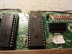
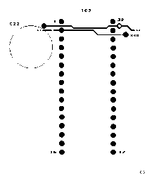
To use JEDEC EPROM for internal ROM:Disconnect IC3 pin 2 from the ROE track by cutting it in two places on the component side of the board. The adjacent A16 track is shown for clarity because the view is usually obscured by a socket. Disconnect IC3 pin 24 from the A16 track by cutting it on the solder side of the board. Connect IC3 pin 24 to the ROE pad close to IC3 pin 17. Connect the ROE pad close to IC3 pin 31 to the ROE track going to SLOT 1. Connect IC3 pin 2 to the A16 track going to SLOT 2.To use 256K JEDEC EPROM for internal ROM:Also disconnect IC3 pin 30 from VCC by cutting the track from pin 31. Connect IC3 pin 30 to the A17 track going to slot 2 pin 36. 128K JEDEC EPROM should still work but is not tested.To use 512K JEDEC EPROM for internal ROM:Also disconnect IC3 pin 31 from VCC by cutting the track from pin 32. Connect IC3 pin 31 to the A18 track going to slot 2 pin 37. Not sure if 128K or 256K JEDEC EPROM can be used after this modification because of pin 31 /PGM. For layout of code on larger than 128K internal ROMs see: Z88 Internal ROM Modifications
Solder side of board.
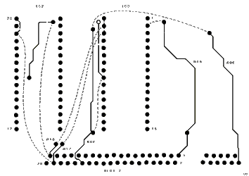
To use 128K static RAM for internal RAM: No track changes needed.To use 512K static RAM for internal RAM:Disconnect IC2 pin 30 from the VCC by cutting the track from pin 32. Connect IC2 pin 30 to A17 at slot 2 pin 36. Disconnect IC2 pin 31 from the /PGM track by cutting it close to the pad near pin 1 and 2. Connect the IC2 pin 31 to A18 at slot 2 pin 37. Not sure if 128K static RAM can be used after this modification because of pin 30 CS2.
De-soldering multi-pin chips is difficult. To make it easier, cut all pins close to the chip and unsolder them one at a time.
Installing the chips in a socket is recommended. A low profile socket is a must. Even so, the keyboard reaction plate may have to be cleared of reinforcement webs like it is above the ROM chip.
There are ultra low sockets that makes the RAM chip fit without clearing the reinforcements. Tested by Per Svensson 21 January
Programming the Flash Chip
There are two main ways of programming the Flash Chip.
Blank Flash chip
you need
- A suitable EPROM Programmer
- Download the latest copy of OZ
or you could send the chip to Rakewell who can program it for you.
Reprogram the Flash chip
Once you have OZ in the Z88 on a flash chip, further updates may be done without removing the chip.
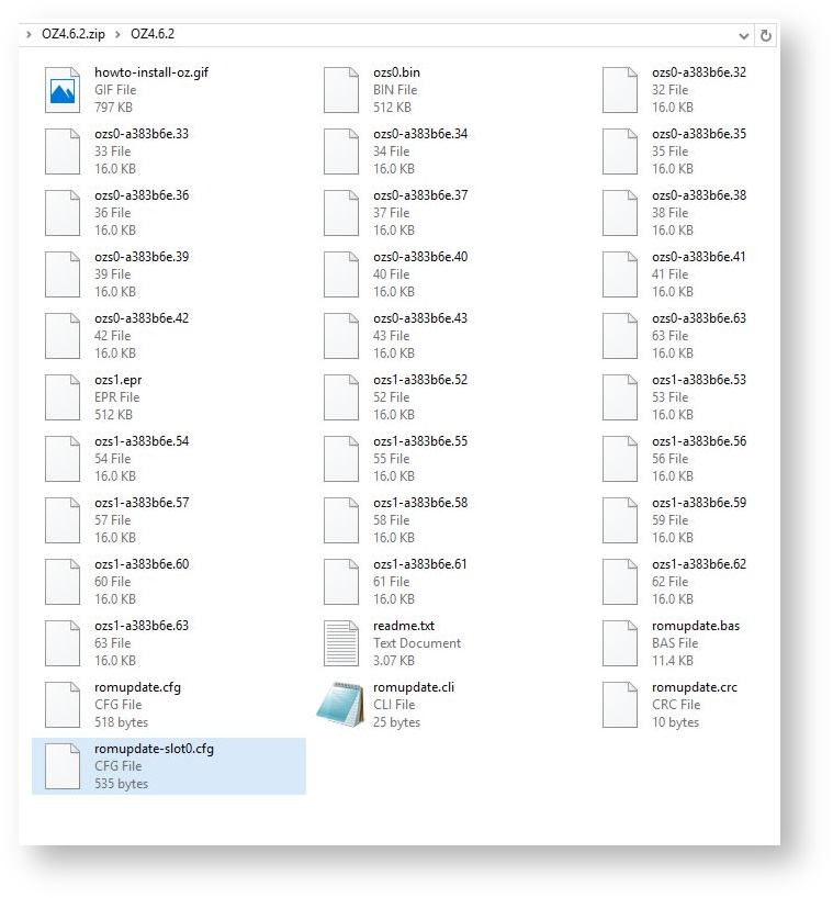
You need to Download the latest copy of OZ from the internet to the Desktop computer. For example, here are the unzipped files of OZ 4.6.2 displayed here.
Unzip the Files
At first sight they appear to be confusing. This is because there are more files than we need. The ones we need are:-
- romupdate.bas (the application to blow the image into the Flash chip)
- romupdate.crc - a file to check the integrity of romupdate.bas
- the image files for Slot 0 - the internal ROM. These start with ozs0-xxxxxxx.32-43 63
- romupdate-slot0.cfg - the file that lists of the files needed to blow the image together with their checksums
- romupdate.cli
Before transferring the files to the Z88, rename romupdate-slot0.cfg to romupdate.cfg.
Using Eazylink2, transfer the files to :RAM.0.
Select the Filer F and mark romupdate,cli with the key,
Issue the EXECUTE command with EX.
After checking that all the files are correct, change the 'Select slot to write bank binaries' to 0
WARNING
Unable to select Slot 0. 1, 2 and 3 work.
or you could send the chip to Rakewell who can program it for you.
