Technical Spec of a Flash and RAM chips
| Z80 4MHz | AS6C8008 | ||||||
|---|---|---|---|---|---|---|---|
Supply Voltage Min | V | 2.4 | 2.7 | 2.7 | 4.5 | ||
| Supply Voltage Typ | V | - | 3.0 | 3.0 | 5.0 | ||
| Supply Voltage Max | V | 5.5 | 5.5 | 5.5 | 5.5 | ||
Input High Voltage | V | 2.2 to VCC | 0.7 x VCC min to VCC+0.3 | 2.2 to VCC+0.3 | 2.4 to VCC+0.3 | 2.4 to VCC+0.5 | 2.2 to VCC + 0.5 V |
Input Low Voltage | V | -0.3 to 0.8 | 0.5 to 0.8 | -0.5 to 0.8 | - 0.2 to 0.6 | - 0.2 to 0.6 | –0.5 to 0.8 |
Output High Voltage | V | 2.4 min | 0.85 x VCC | 2.4 min | 2.4 min | 2.4 min | |
Output Low Voltage | V | 0.4 max | 0.45 | 0.4 max | 0.4 max | 0.4 max | |
Standby Power | uA | 1 | 3.5 to 50 | 6 to 80 | 10 to 50 | 2 to 8 | |
| Power Consumption | mA | 20 - 40 | 39 | 60 | 30 to 60 | 1.8 to 3 | |
VCC for Data Retention | V | 1.5 | 2.0 | 1.5 | 2.0 | ||
| Read Timings | |||||||
| Read Cycle Time tRC | ns | 55 min | 55 min | 55 min | 55 min | 45 min | |
| Address Access Time tAA | 55 min | 55 max | 55 max | 55 max | 45 max | ||
Chip Enable Access Time tACE | 55 min | 55 max | 55 max | 55 max | 45 max | ||
| Output Enable Access Time tOE | 30 max | 25 max | 30 max | 30 max | 22 max | ||
| Chip Enable to Output in Low-Z tCLZ | 18 min | 10 min | 10 min | 10 min | 5 min | ||
| Output Enable to Output in Low-Z tOLZ | 18 min | 10 min | 5 min | 5 min | 10 min | ||
| Chip Disable to Output in High-Z tCHZ | 30 max | 20 max | 20 max | 18 max | |||
Output Disable to Output in High-Z tOHZ | 25 max | 20 max | 20 max | 18 max | |||
Output Hold from Address Change tOH | 0 | 10 min | 10 min | 10 min | 10 min | ||
| Write Timings | |||||||
Write Cycle Time tWC | 55 min | 55 min | 55 min | 55 min | 45 min | ||
Address Valid to End of Write tAW | 40 min | 40 min | 50 min | 50 min | 35 min | ||
Chip Enable to End of Write tCW | 0 | 50 min | 50 min | 35 min | |||
Address Set-up Time tAS | 0 | 40 min | 0 | 0 | 35 min | ||
Write Pulse Width tWP | 20 min | 30 min | 45 min | 45 min | 35 min | ||
Write Recovery Time tWR | 0 | 0 | 0 | 0 | |||
Data to Write Time Overlap tDW | 25 min | 25 min | 25 min | 25 min | 25 min | ||
Data Hold from End of Write Time tDH | 0 | 0 | 0 | 0 | 0 | ||
Data Setup to Write End | 25 min | ||||||
Output Active from End of Write tOW | 5 min | 5 min | 5 min | ||||
Write to Output in High-Z tWHZ | 25 max | 20 max | 20 max | 10 max | |||
| THE Z80 CPU : TIMING |
This is the exchange between Rakewell and LYONTEK to find out why their RAM chip fails.
LYONTEK - LY62W10248ML-55LLI - SRAM, 8M, 1MX8, 2.7-5.5V, 44TSOPII This memory chip should be a 'drop-in' replacement for the BSI chip. TESTED FAILS when loading a file in PipeDream. Manufacture response:-
My response :-
Manufacture response:-
|
My response
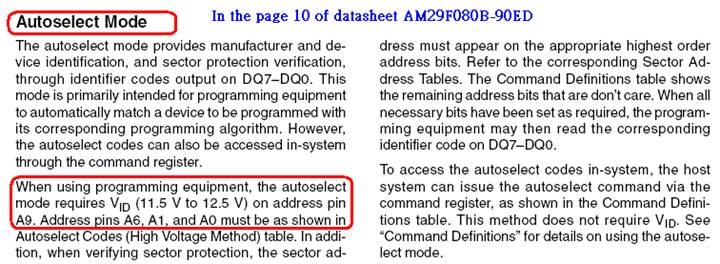
Note: FYI The Z88 has 3 slots for these cards. It can only program EPROMs using the 12v line in slot 3. The RAM fails when the card is in Slot 1, there is no 12v line available there. We do use the auto-select mode to see what Flash chip is present on the card. We also program the Flash chip. We do not use the higher voltage to do these functions. We use the alternative mode so that we can program the card in any slot using 5v. I can confirm that I have programmed the Flash Chip and read it. The card does not fail when I do that.
The Z88 recognizes that it has RAM. I have a simple RAM test, which passes.
I have uncompressed files, and have saved files to the flash chip. The failure occurs when I am loading a larger file into the word-processor. The Z88 displays a “fail” message which is associated to a memory failure of some sort (usually if the RAM is removed from the slot).

