Z88 Hardware Investigation
Check Rules on Flash Chip
The aim of this section was to override the software commands with hardware changes. The main differences, were not so much the software commands but the Flash chip would write to the data bus irrespective of the hardware controls.
Motherboard
The following signals are generated on the motherboard. Some of them are used on the External Card.
Z80 Processor
The Z80 processor uses two circuits.
- to refresh and use the RAM and
- I/O circuits.
The Z88 uses these separate circuits, using RAM in one and the ROM into the other. It selects these by using two hardware signals generated by the BLINK IC 4,
ROE and POE
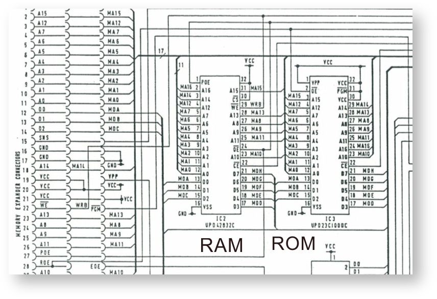
The Z88 circuit shows the internal ROM and RAM are using,
- ROE for the ROM
- POE for the RAM
These Output Enable (OE) signals are used to enable the RAM or ROM onto the data bus.
Negative signals
ROE and POE are negative true signals. i.e. when they are at 0v, they are enabled. Normal convention would dictate that they should be written as /ROE and /POE but as the Z80 data sheet uses this format with OE when it should really be /OE.
Memory Addressing
Memory address lines are generated by the Z80 and are used to select which Slot to use.
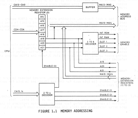
The memory addressing of the Z80 (CA0 - CA15) is expanded for the Z88 MA0 - MA 21) using
- a buffer using signals from the Z80 and
- one of four Memory Extension Registers
The notation is.
- CA xx is the output from the Z80
- MA xx is the output from the Z80 and memory extension register that go to all the expanded 4 slots
- A xx are internal address lines within the memory expansion section.
Buffered
These signals, buffered from the Z80, go to all the slots.
CA0 - CA13 become MA0 - MA13
Latched Memory Extension Registers
CA14 - CA15 are used via a decoder, to ENABLE the outputs 1 of 4 latches. The value written into each latch is written by the Z80 via the data bus
The next 8 expanded address lines are generated by 4 latches,
A14 - A19 become MA14 - MA 19 goes to all slots.
Enable the slot
A19 - A21 are used via a decoder to enable
- Slot 0 IPCE ROM 512K
- Slot 0 IRCE RAM 512K
- Slot 1 SEI (30) 1M
- Slot 2 SE2 (30) 1M
- Slot 3 SE3 (30) 1M
The number in brackets is the Pin number of the external card connector.
Testing & Tools developed
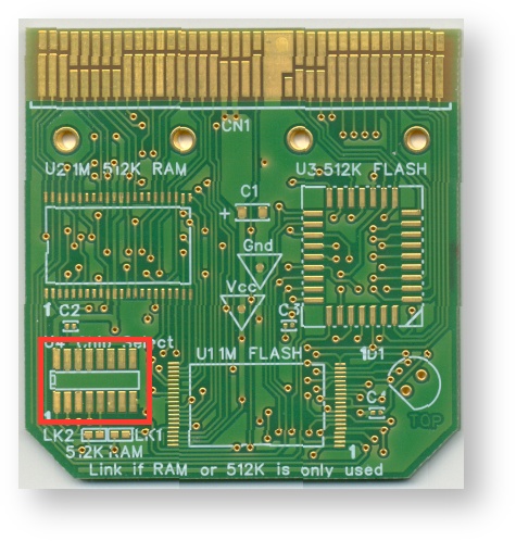
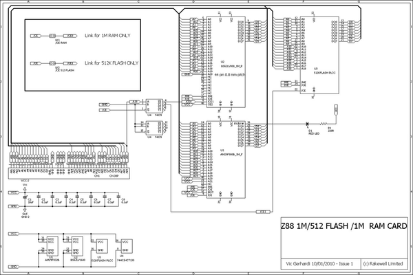
The 512K/512K Flash Circuit
This circuit was drawn up by looking at what Cambridge Computer were doing with their memory cards, without understanding the significance of POE and ROE. As a result only ROE was used for both the RAM and Flash.
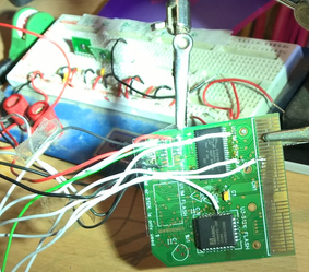
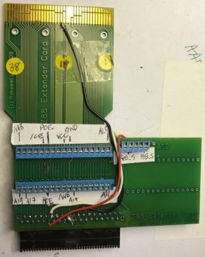
Extender & 512K/512K Flash Card
| Wiring on the Extender and 512K/512K Card | |
|---|---|
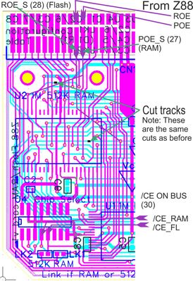
Signals used
| OUTPUT ENABLE SECTION | ||||||
|---|---|---|---|---|---|---|
| Output signals from the Z88 | Input signals to the External Card | |||||
| ROM | ROE (28) | |||||
| RAM | POE (27) | |||||
| ROE_S (/OE TO RAM) | ||||||
| POE_S (/OE TO FLASH) | ||||||
| DECODING SECTION | ||||||
| C ENABLE | /CE (30) | |||||
| CE_RAM | CE_FL | |||||
RESULTS
POE & ROE
It was initially thought that these Output Enable signals would be able to select the RAM (POE) and ROM/FLASH (ROE) independently.
Unfortunately, they are in phase, so the only advantage in using POE is if the Z88 used dynamic RAM. Static RAM is now used, so ROE may be used for both the RAM and Flash.
Cambridge Computer Memory Cards /OE Signal
Which /OE signal did CC use on their memory cards? POE or ROE?
This can be tested by connecting either POE_S or ROE_S to 5v which would disable the OE to the chip. During a HARD RESET the Z88 sees how much RAM is there. It will only see it when the correct OE is selected.
This test was not done, as we ran out of time. The Z88 found the RAM irrespective on which Output Enable the RAM was connected to. A card with LED showing the state of the control lines could be built, ROE POE WE CE if it was felt that this information was useful.
| Signal | Size |
|---|---|
| 32K RAM | |
| 128K RAM | |
| 512K RAM | |
| 1024K RAM | |
| 32K EPROM | |
| 128K EPROM | |
| 256K EPROM |
Results
Unexpected Result - Flash Write
Two tests were run at different times. Taking out the decode, the RAM and Flash chips were tested separately using ether the /CE line connected to the RAM or the Flash.
After doing a HARD RESET the RAM was found and recognised in CARD. When running Flash Test, it actually recognised the Flash chip even though /CE the hardware Chip Enable pin was connected high.
There are several different ways the Flash chip can be written to. Due to RAM and ROM being on the same bus, both the hardware and software engineers need to ensure that the /CE signal is respected, otherwise the Flash may write when the RAM is being accessed.
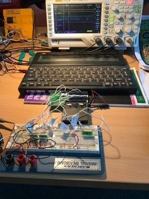
Oscilloscope traces (to be continued)
It has been quite a job getting a stable platform to do reliable testing. Today has been the first time that
- none of the wires fell off the breadboard,
- the signal wires have been lengthened and labeled
- we remember that
- ROE is the output for FLASH and
- POE is the output for RAM.
Running Flash Test
- CE is SE3 - Generated by the latch - which is connected to /CE Flash chip
- POE - Generated by the Z80 - which is the /OE for the RAM
- ROE - Generated by the Z80 - which is connected to /OE Flash chip
- WE - Generated by the Z80 - which is connected to /WE Flash chip
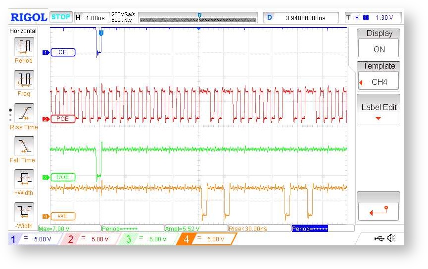
READ
When CE is selected reading to the chip is as expected.
- WE is high
- CE goes low
- ROE goes low during
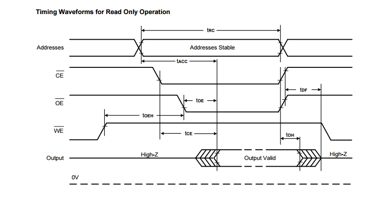
Compare traces in the datasheet.
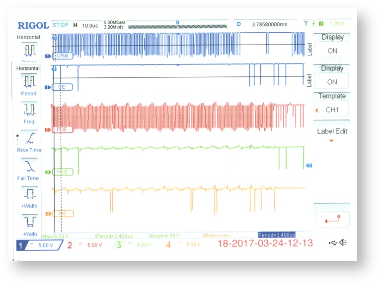
PROGRAM OPERATION i.e. Writing to the Flash chip
This shows the internal RAM being accessed
- CRA1 Internal RAM
- CE Card Enable
- POE Output Enable for RAM
- ROE Output Enable for Flask
- WE Write Enable
All enable signals are LOW.
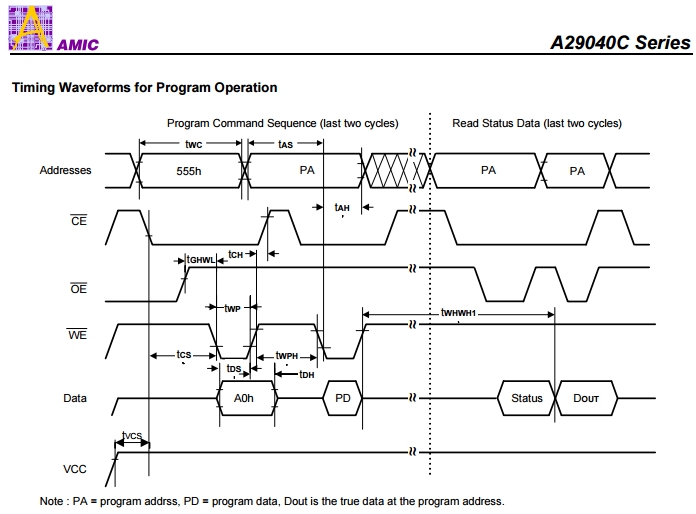
No CE signal during command mode
The diagram above shows /CE being selected when the 555h address is on the address bus. This is not being shown on the oscilloscope readings. The /CE go down when the Flash card is being returned to the ROM mode
Conclusion
RAM Chips
Read/Writing to RAM chips, all signals are respected
Reading Flash Chip
When reading a Flash Chip, all signals are respected.
Writing to Flash Chips
This is where it goes wrong. - see above
Flash CE Chip Enable
When the CE signal was set high, i.e. disabling the chip, Flashtest reported that it had found the Flash chip. This means that some of the flash chip commands used, do not respect the chip enable hardware controls.
POE & ROE
Only ROE has been used to output enable both the RAM and Flash on the card. Separating them so that POE goes RAM and ROE to Flash has not improved its performance.The differences in the traces show the additional cycles in POE to refresh the RAM. This facility, provided by the Z80, was so that dynamic RAM could be used. The RAM used by Cambridge Computer were Pseudo static RAM (which was dynamic RAM, but from the outside world looked like static RAM). The RAM now used is static RAM, these refresh cycles are no longer needed.
Both signals are in phase, so the initial assumption that we could use 1M Flash and 1M RAM was incorrect. A decoder is still needed to address the 1M memory space to the devices on the card.
Solutions
Software
If software changes are implemented the following points maybe considered.
SE 1 Slot Enable 1, 2 or 3
At the moment, when a command is sent to a flash chip, that command is read and actioned by all the flash chips that are in the Z88. This is because the CE on the flash chip is either not sent at the correct time or is dis-respected.
Is this because it is not generated by
- a call in the program or
- incorrect setting of SE1 in the Memory Extension Registers (unlikely as 1M RAM works)
Other signals are generated go to all the chips.
| Signal | Type | Generated by | |
|---|---|---|---|
| MA0 - MA11 | Address | Z80 | 555h |
| POE & ROE | Control | Z80 & U4 | |
| WE | Control | Z80 | |
| D0 - D7 | Data | Z80 | |
| SE1 | Control | Memory Extension Registers | |
| MA14 - MA21 | Address | Memory Extension Registers |
MA14 - MA21 are correct as the slots can address 1M Flash and RAM chips.
Write Protected Area
I am no longer sure that using write protect will solve the problem.
If the Write Protected area was set to the top 256K, where OZ 4.7 resides, the flash chip would regard this area as ROM which maybe desirable.
All commands that turn off the write protect areas should be modified so that the write protected area continues to be respected.
Other applications will need to be modified to add the write protected area after updating software if users are able to update their flash cards. These include
- ROMUpdate and
- ROMcombiner
- Update software in OZ 4.7.
Chip id
When reading what flash chip is in the Z88, and whether the application will run, only the Primary information the Device ID (90h x01h) is considered. If the manufacture ID, size of device and other information is regarded as secondary information for information only, this would future protect devices. Other different manufacture, size of chips used, may be changed without needing any software changes. The size of the chip could be decided using the algorithm used in the case of determining the size of the EPROM card.
Hardware
This is covered in a separate section. See Hardware Modification Options Unfortunately, the modifications did not resolve the problem due to /CE is not enabled when sending software commands.
